
VLSI Chip Design Course in Visakhapatnam | Of course. Here is a full, detailed explanation of a VLSI Chip Design Course, covering its significance, target audience, the complete design flow, key skills, and career paths.
What is a VLSI Chip Design Course?
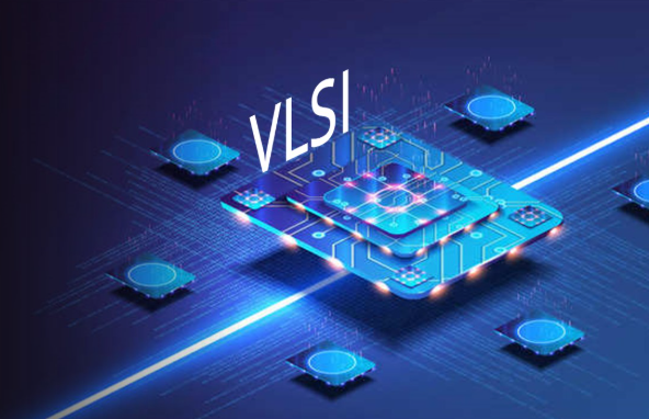
VLSI Chip Design Course in Visakhapatnam | A VLSI (Very Large-Scale Integration) Chip Design course is a specialized program that teaches the principles and practices of designing integrated circuits (ICs) by combining millions or billions of transistors onto a single silicon chip. It encompasses the entire process, from conceptualizing the system’s functionality to creating the geometric patterns (layouts) used for semiconductor fabrication.
This field sits at the intersection of Electrical Engineering, Computer Science, and Physics.
Who is this Course For?

Electronics/Electrical Engineering (ECE) Students & Graduates: The primary audience, providing the necessary foundation in semiconductor physics and digital systems. VLSI Chip Design Course in Visakhapatnam | Computer Science/Engineering Students: Particularly those interested in computer architecture, hardware-software co-design, and using programming to automate design processes. Embedded Systems Engineers: Looking to understand the hardware on which their software runs at the deepest level. Professionals in Related Fields: Seeking to transition into the semiconductor industry. R&D Engineers: Working on cutting-edge technologies like AI accelerators, IoT chips, and high-performance computing.
Core Components & Syllabus: The VLSI Design Flow A comprehensive course is structured around the IC design flow, which is a sequence of steps to create a chip.VLSI Chip Design Course in Visakhapatnam | The following chart illustrates this rigorous process, from system conception to final packaging:
Part 1: Front-End Design (The “What” the Chip Does) This phase defines the chip’s functionality and logic. Digital Logic Fundamentals: Boolean algebra, combinational and sequential logic (gates, flip-flops, finite state machines).
Hardware Description Languages (HDLs): The core of front-end design. Verilog & SystemVerilog: Learning to code the behavior and structure of digital circuits. This is like software programming for hardware. System
Architecture & Microarchitecture: Top VLSI Chip Design Course in Visakhapatnam | Defining the high-level structure (e.g., how a CPU pipeline will work) based on performance, power, and area (PPA) goals. Functional Verification: Ensuring the HDL code behaves as intended. Simulation: Using tools like ModelSim/VCS to test the design with different stimuli (testbenches). Best VLSI Chip Design Course in Visakhapatnam | Universal Verification Methodology (UVM): A systematic framework for creating robust and reusable testbenches (advanced topic).

Part 2: Back-End Design (The “How” the Chip is Built) This phase transforms the logical description into a physical layout ready for manufacturing.Best VLSI Chip Design Course in Visakhapatnam | Logic Synthesis: Using tools like Design Compiler to automatically convert the HDL code into a gate-level netlist (a list of standard cells like AND, OR, flip-flops and their connections). Design for Testability (DFT): Incorporating structures like Scan Chains into the design to allow for testing the manufactured chip for fabrication faults. Physical Design (The most intensive part): Floorplanning: Top VLSI Chip Design Course in Visakhapatnam |Defining the overall size and layout of the chip, placing major blocks and I/O pads. Placement: Determining the exact location of each standard cell on the die. Clock Tree Synthesis (CTS): Building a network to distribute the clock signal evenly across the chip to prevent skew. Routing: Automatically connecting the placed cells with metal wires using tools like Innovus/ICC2. Physical Verification:Best VLSI Chip Design Course in Visakhapatnam | DRC (Design Rule Check): Ensuring the layout adheres to the foundry’s manufacturing rules. LVS (Layout vs. Schematic): Verifying that the physical layout matches the original gate-level netlist. Timing Analysis: Performing final sign-off checks to ensure the chip will run at the desired speed (using PrimeTime).
Part 3: Supporting Concepts & Technologies CMOS Technology: Understanding the transistor (MOSFET) as the fundamental building block.
Analog & Mixed-Signal Design (Basics): Introduction to designing critical analog components like Phase-Locked Loops (PLLs), data converters (ADCs/DACs) that exist on mostly digital chips.Low-Power Design Techniques: Crucial for mobile and IoT devices.Best VLSI Chip Design Course in Visakhapatnam | Methods include clock gating, power gating, and multi-voltage domains.EDA Tools: Hands-on experience with industry-standard tools from vendors like Synopsys, Cadence, and Siemens EDA. Key Features & Benefits of Learning VLSI Design High Demand & Specialization: The global semiconductor shortage has skyrocketed the demand for skilled VLSI engineers.Intellectual Challenge: Work at the cutting edge of technology, pushing the limits of physics to create powerful and efficient electronics. Top VLSI Chip Design Course in Visakhapatnam |Diverse Career Paths: The field offers specialization in front-end, back-end, verification, analog design, and architecture.Impactful Work: You design the “brains” behind every electronic device, from smartphones and laptops to medical equipment and cars.
Challenges & Important Considerations Steep Learning Curve: Requires a strong foundation in digital electronics, semiconductor physics, and scripting/programming. Cost of Tools: Professional EDA tools are extremely expensive. Best VLSI Chip Design Course in Visakhapatnam |Courses often use academic licenses or open-source tools like OpenROAD for practical work.Rapidly Evolving Field: Requires continuous learning as process technology shrinks and new challenges emerge.What to Look for in a Good VLSI CourseStructured Curriculum: Must cover the complete flow from HDL to GDSII (the final layout file). Hands-On Projects: The cornerstone of a good course. Best VLSI Chip Design Course in Visakhapatnam | You should complete a project where you design a small circuit (e.g., a microprocessor core, an encryption engine) through key stages like RTL coding, synthesis, and physical design.Industry-Standard EDA Tools: Access to tools from Synopsys, Cadence, or Mentor Graphics is a significant advantage.Experienced Instructors: Faculty or instructors with industry experience can provide practical insights beyond textbook theory. Focus on Scripting: Automation is vital. VLSI Chip Design Course in Visakhapatnam | The course should encourage the use of Tcl, Perl, or Python for tool interaction and task automation. Career Paths after a VLSI Course RTL Design Engineer: Codes the HDL for specific blocks of the chip.
Verification Engineer: Develops testbenches and scenarios to ensure design correctness (a very high-demand role).
Physical Design Engineer: Performs the place-and-route and sign-off for timing and power.CAD Engineer: Develops and supports the flow and automation scripts for the design team. Best VLSI Chip Design Course in Visakhapatnam |ASIC/FPGA Engineer: Implements designs on either Application-Specific Integrated Circuits (ASICs) or Field-Programmable Gate Arrays (FPGAs).
Conclusion: A VLSI Chip Design course is a challenging but immensely rewarding gateway into the heart of the modern technological world. Top VLSI Chip Design Course in Visakhapatnam |It provides the specialized knowledge and practical skills to create the complex integrated circuits that power our digital lives.For an engineer, there are few fields more fundamental and impactful than VLSI, offering a career at the forefront of innovation in the multi-billion dollar semiconductor industry.

The chip design includes different types of processing steps to finish the entire flow. For anyone, who just started his career in VLSI industry has to understand all the steps of the VLSI design flow. Best VLSI Chip Design Course in Visakhapatnam | Each and every step of the VLSI design flow has a dedicated EDA tool that covers all the aspects related to the specific task perfectly.All the EDA tools can import and export the different file types to help making a flexible VLSI design flow that uses multiple tools from different vendors.The VLSI design flow is shown in the figure below.
System Specification
- The first step of VLSI Design Flow is system specifications. Top VLSI Chip Design Course in Visakhapatnam | System specification is a high level representation of the system. The factors to be considered in this process include performance, functionality and interface.
Architectural Design
- This is step where main work start with the help of system specification.
- Design engineer design the architecture according to system specification.
Functional and Logic Design
- In this step functionality of design are identified.
- It specify the hardware implementation of system functionality.
- The outcome of functional design is usually a timing diagram.
- In logic design step,register allocation, logic and arithmetic operations of the design that represent the functional design are derived and tested this description is called RTL description. VLSI Chip Design Course in Visakhapatnam | RTL stands for register transfer level.In this step, system specification is expressed in hardware description language (HDL) such as Verilog and VHDL.
- RTL description is used for simulation to test the functionality with the help of EDA tools.
- Functional verification is performed to ensure the RTL design is done according to the specifications
- RTL code is converted to gate level netlist using synthesis tools. Netlist is a description of the circuit in terms of gates and connections between them.
- To verify whether the synthesis tool has correctly generated the gate-level netlist a verification should be done.

Circuit Design
- In this step circuit is designed based on the logic design. Best VLSI Chip Design Course in Visakhapatnam |The Boolean expressions are converted into circuit representation by taking into consideration the power and speed requirement of original design.
- Circuit simulation is used to verify the correctness and timing of each component.
- Diagram consists circuit elements such as gates and transistors.
Physical Design
- In this step the netlist is converted into physical geometric representation.
- Layout is representation of an IC in terms of planar geometric shapes which correspond to the patterns of metal oxide or semiconductor layers that make up the components of the Integrated circuit. Layout is designed by eda tool such as cadence virtuoso.
- Physical design is a very complex step therefore it is divided into sub steps such as floor planning, placement, clock tree synthesis, routing etc and timing analysis checks are formed in each and every step during physical design.
- Floor planning which is a process of placing the various blocks and the I/O pads across the chip area based on the design constraints.
- Placement of physical elements within each block and integration of analog blocks or external IP cores is performed. VLSI Chip Design Course in Visakhapatnam |
- When all the elements are placed, a global and detailed routing is running to connect all the elements together.
- Output of layout is GDSII file which is given to the foundry to fabricate the chip. The layout should be done according to foundry design rules.
Physical Verification and Signoff
- In this step we perform physical verification checks such as Layout Vs schematic (LVS) and Design Rule check (DRC).
- DRC verifies whether the given layout satisfies the design rules provided by the fabrication team. DRC checks are nothing but physical checks of spacing rules between metals, minimum width rules, via rules etc.
- LVS is a major check in the physical verification stage. Top VLSI Chip Design Course in Visakhapatnam | Layout is compared with the schematic for verifying whether their functionally match or not. If match, then the LVS reports clean.

Fabrication
- After physical verification step the design is ready for fabrication. Best VLSI Chip Design Course in Visakhapatnam | Tape out is the final result of the design process for integrated circuits before they are sent for manufacturing. The tape-out is specifically the point at which the graphic for photo mask of the circuit is sent to foundry.
- Fabrication process consists of several steps involving wafer growth, epitaxial growth masking, etching, doping, deposition, and diffusion of various materials on the wafer. During each step one mask is used.
Packaging and Testing
- Each of the wafers contains hundreds of chips. These chips are separated and packaged by a method called scribing and cleaving. Best VLSI Chip Design Course in Visakhapatnam | The chips that are failed in electrical test are discarded.
- Each chip is packaged and tested to ensure that it meets all the design specifications and functions properly.